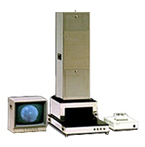
This is the well known technology, called as “Magic Mirror” or “Makyo Inspection system” to be able to inspect semiconductor wafer surface for latent damages. Non-contact and non-destructive test method. It can be used for Si Wafer, GaAs wafer, Polished flat Glass surface, Sapphire wafer, semi-transparent wafer surface, polished metal surface and many others. Optics requires no maintenance and lamp has to be replaced for a maintenance. Other options, such as automated damage inspection software and printer options.
|
Features
Applications ◇ Wafer surface inspection |
 |
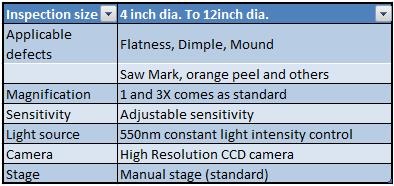
■Standard Specification
Inspection size 4 inch dia. To 12inch dia. Applicable defects Flatness, Dimple, Mound Saw Mark, orange peel and others Magnification 1 and 3X comes as standard Sensitivity Adjustable sensitivity Light source 550nm constant light intensity control Camera High Resolution CCD camera Stage Manual stage (standard)
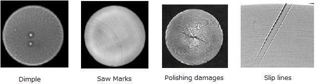
■Example of images of wafers
■Available options
◇ Motor controlled rotating inspection stage
◇ Automated Defect Detection Image Processing Software
◇ Screen Image Printer
◇ Wafer handling robot and wafer transfer system
Note: Demonstration of Magic Mirror is available on request at our factory. We welcome your samples and we are more than happy to inspect samples